PLL based ULA
PLL based ULA
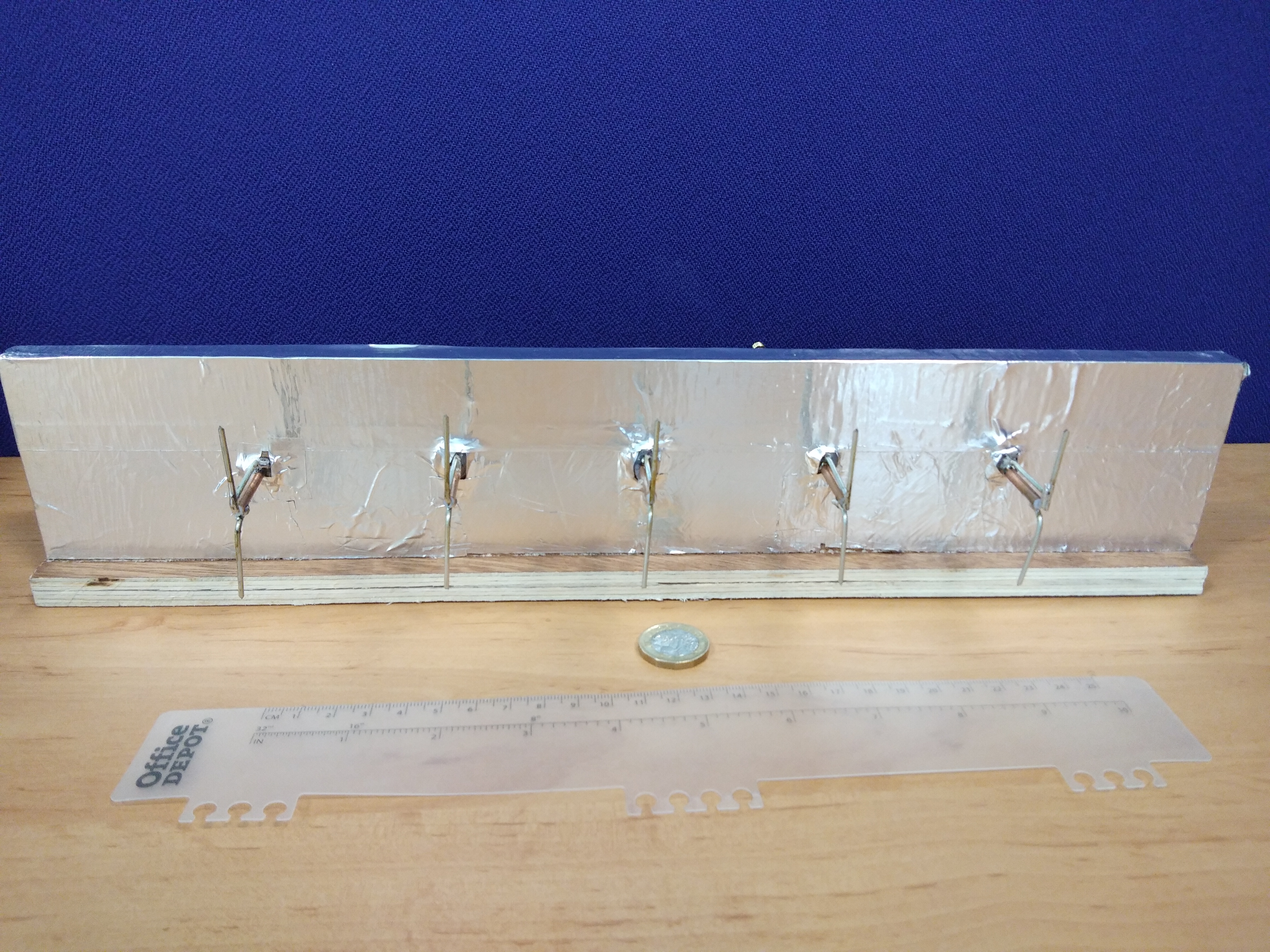
Hardware

Each PCB contains 5 LTC6946 PLLS. Each PLL shares the same 10MHz source.
In order to be able to adjust the output phase of each PLL the square wave 10MHz reference is put through a low pass filter with a varactor. By changing the voltage on the varactor the rise time of the square wave is adjusted moving the point at which the PLL locks on to the reference. This voltage is output from a DAC on the STM32F051 microcontroller
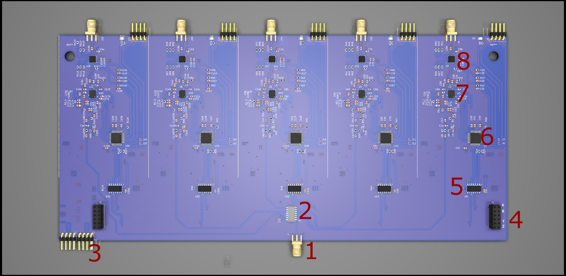
| Reference | description | link |
|---|---|---|
| 1 | 10 MHz reference input | |
| 2 | Hex invertor reference buffer | 74HC04 |
| 3 | Power input | |
| 5 | RS-485 transceiver | MAX3089 |
| 6 | Microcontroller | STM32F051K4Tx |
| 7 | PLL | LTC6946IUFD-4-PBF |
| 8 | Attenuator | DAT-15R5A-SP+ |
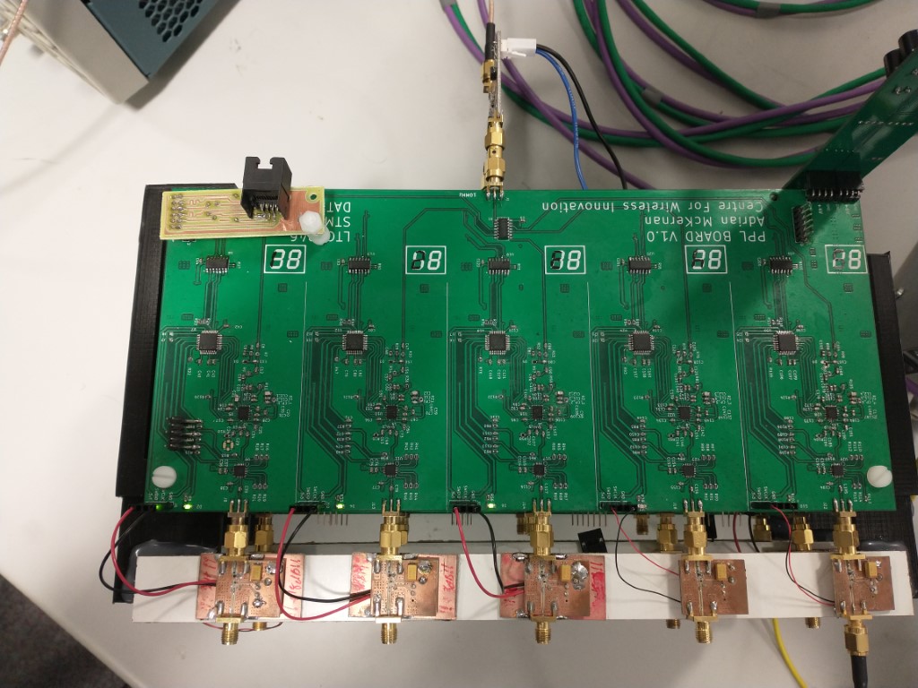
The PCB was designed in KiCAD and is available here.
A pdf of the schematic for the main board can be found here .